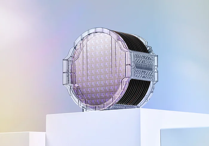


The 3nm Pessimism Wall – Hidden Costs in Advanced Semiconductor Design
31. March 2024
Power electronics: The driving force behind EVs
10. January 2025
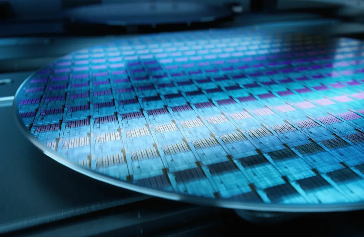
As semiconductor design enters the 3nm era, much of the industry’s focus is on architecture, performance, and power efficiency. However, an often-overlooked factor is becoming increasingly critical: wafer sourcing and material quality.
While design methodologies struggle with challenges such as the “pessimism wall” and shrinking margins, the physical foundation of every chip—the wafer itself—plays a decisive role in determining real-world performance.
Why Wafer Quality Matters More at 3nm
At advanced nodes, design margins are already under pressure. Any additional variability introduced at the wafer level directly impacts:
- Timing stability
- Power consumption
- Yield and reliability
Parameters that were once considered manageable—such as thickness variation (TTV), flatness, or surface quality—now have a significantly stronger influence on device behavior.
At 3nm, even small deviations can lead to measurable performance differences.
The Link Between Design Margins and Material Variability
Modern chip design often compensates for uncertainty by adding conservative margins. But not all uncertainty originates from design models—some of it comes from material variation and process inconsistencies.
Key wafer-related factors include:
- Uniformity: Variations in thickness or doping can affect electrical characteristics across the wafer
- Surface quality: Defects or particles can reduce yield, especially in highly scaled geometries
- Thermal oxide consistency: Variations impact device reliability and performance
- Batch-to-batch stability: Inconsistent supply increases the need for additional design guard bands
Reducing variability at the wafer level can therefore directly help minimize unnecessary design margins.
Supply Chain Pressure at Advanced Nodes
At 3nm, the semiconductor supply chain becomes more complex and less flexible:
- Limited number of qualified manufacturers
- Higher qualification requirements
- Longer lead times and tighter specifications
This makes reliable sourcing and strong supplier networks more important than ever. Delays or inconsistencies in wafer supply can impact not only production schedules but also design validation and ramp-up phases.
A Strategic Approach to Wafer Sourcing
To support advanced-node projects effectively, companies need to rethink how they approach wafer sourcing:
- Work with qualified and proven manufacturers
- Ensure tight specification control and traceability
- Secure flexible supply options to manage demand fluctuations
- Align wafer specifications with actual design requirements—not just standard values
Close collaboration between design teams, fabs, and suppliers is essential to reduce risk and improve overall efficiency.
How ABC GmbH Supports Advanced Node Projects
At ABC GmbH, we specialize in sourcing high-quality silicon wafers through a global network of qualified manufacturing partners.
Our approach focuses on:
- Flexibility: Tailored wafer specifications based on customer requirements
- Quality assurance: Strict supplier qualification and traceability
- Global sourcing: Access to multiple manufacturing sources to ensure supply stability
- Value-added services: Including coatings, reclaim, thinning, cutting, and marking
This enables our customers to reduce variability, improve process stability, and support advanced-node performance targets.
Conclusion
At 3nm and beyond, semiconductor performance is no longer defined by design alone. Material quality and supply chain reliability have become key success factors.
Reducing variability at the wafer level helps minimize design uncertainty, enabling better performance, higher yield, and lower overall cost.
In an environment where margins are already under pressure, the right wafer sourcing strategy can make a measurable difference.