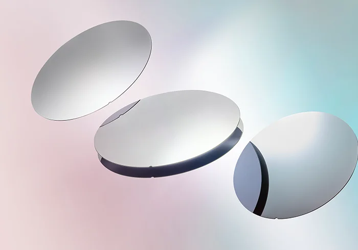


SOI Wafer
SOI-Wafer
SOI wafer (Silicon on Insulator Wafer) form the foundation of modern semiconductor technology and enable innovations across numerous high-tech sectors.
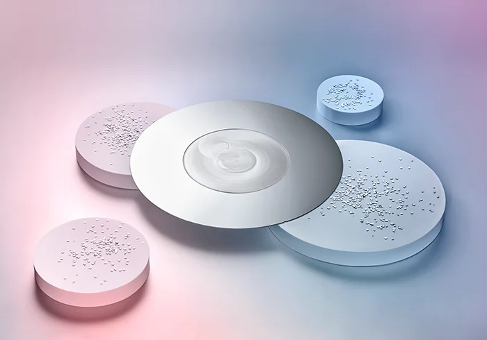
Active Business Company GmbH offers SOI wafer, double-bonded SOI wafer, and triple-bonded SOI wafer in a wide range of specifications. These include thick-film SOI wafers with a device layer thickness of >2 µm and thin-film SOI wafers with a device layer thickness of <2 µm. We provide diameters from 3” to 12” and various thicknesses to meet individual requirements.
Our wafers are the perfect foundation for your projects – from prototypes to mass production. They meet the highest quality standards and are ideal for applications in the automotive, aerospace, mechanical engineering, optics, semiconductor, medical technology, and research industries.
What is a SOI Wafer?
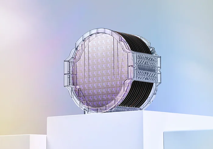
This structure enables outstanding electrical insulation, minimized parasitic effects, and improved device performance. As a result, SOI wafers are indispensable for high-performance applications in microelectronics, sensors, and other high-tech industries. SOI wafers consist of three essential layers:
Device Layer
the active silicon layer containing electronic components.
Buried Oxide (BOX)
the insulating intermediate layer made of silicon oxide.
Handle Wafer
the supporting silicon layer providing stability.
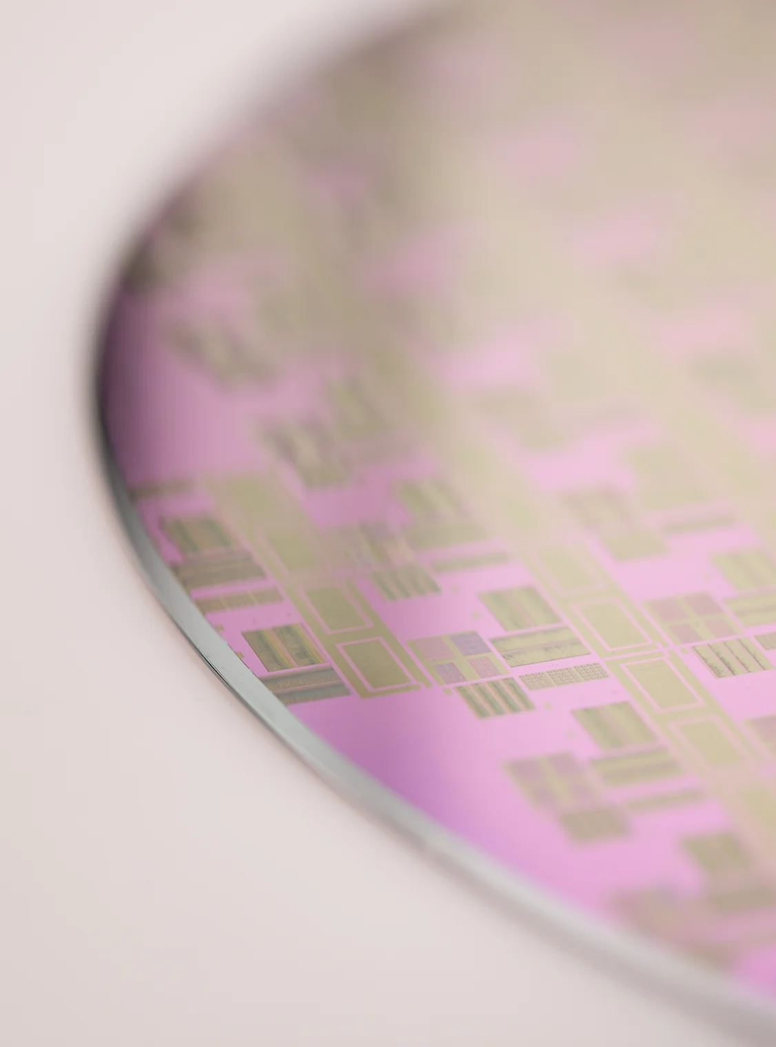
Our SOI Wafer specifications
We deliver wafers precisely according to your specifications – from standard sizes to fully customized solutions. Our experts are happy to advise you on the different wafer types and help you find the optimal solution for your application.
1. Thick-Film SOI Wafer
Thick-film SOI wafers are produced by bonding and polishing two oxidized silicon discs.
- Diameter: 3” to 12”
- Device Layer Thickness: 2 µm to 500 µm and beyond
- Buried Oxide (BOX): 0.1 µm to 5 µm
- Handle Wafer Thickness: 250 µm to 725 µm
Advantages:
- High mechanical stability
- Flexible layer thickness adjustments
- Ideal for MEMS, power semiconductors, and optical applications
2. Thin-Film SOI Wafer
Thin-film SOI wafers are produced using the SIMOX process (Separation by IMplantation of OXygen), in which oxygen ions are implanted and thermally processed into an oxide layer.
- Diameter: 6” to 8”
- Device Layer Thickness: 0.05 µm to 2 µm
- Buried Oxide (BOX): 0.05 µm to 5 µm
- Handle Wafer Thickness: 250 µm to 725 µm
Advantages:
- Maximum purity through SIMOX technology
- Excellent electrical insulation
- Optimal for RF devices, microprocessors, and high-frequency applications
Technological advantages and future
potential of SOI Wafers
Technological advantages of a SOI Wafer
The insulating BOX layer reduces power consumption and minimizes heat generation. This leads to higher energy efficiency and extends the lifespan of electronic components.
Efficient solutions for innovative applications
Thanks to their technological properties, SOI wafers are the ideal solution for high-performance semiconductors such as microprocessors and RF devices. They play a crucial role in 5G-Technology and the Internet of Things (IoT).
Future potential in High-Tech industries
SOI wafers are becoming increasingly important for high-performance sensors, which are essential in autonomous vehicles, medical devices, and industrial applications. Their precision and stability meet the growing demands of modern technologies.
SOI wafer offer significant advantages over conventional silicon wafers.
Application areas for SOI Wafers
Our high-quality wafers are used in numerous industries, including:
- Automotive & Aerospace: Sensors, control systems, and microcomponents
- Mechanical Engineering: Precision components and microsystem technology
- Optics & Watch Industry: Optical sensors and precision components
- Semiconductor Industry: MEMS, RF devices, IGBTs, and power semiconductors
- Medical Technology: Components for diagnostic and therapeutic devices
- Research & Development: Universities, Fraunhofer Institutes, and laboratories
With our broad product portfolio and the ability to manufacture customized special wafers, we offer the ideal solution for demanding applications.
Why choose ABC GmbH?
-
Top Quality:
Silicon wafers from leading international manufacturers -
Flexibility:
Solutions for small and large production volumes -
EU-Based Supply:
Duty-cleared goods with fast, free delivery -
Personal Consultation:
A dedicated contact person for your specific needs -
Full-Service Offering:
Since 2006, we have provided a wide range of services - including coating and dicing - through our extensive, global, and continually growing network, which includes renowned top-tier manufacturers.
Unsere SOI Wafer – Ihre Benefits
SOI Wafer steigern die Effizienz und Lebensdauer von Bauteilen durch hervorragende Isolation und reduzierte Wärmeentwicklung. Sie sind ideal für innovative Anwendungen in High-Tech-Branchen wie Automotive, Medizintechnik und Halbleiter.
Request SOI wafers now.
Our customers’ success is our success. We stand for direct communication, personal consultation, and strong partnerships. We would be happy to provide you with a customized quote.
ABC GmbH is your supplier for silicon wafers and specialized solutions. As a trusted partner in the semiconductor industry, we offer high-quality products and tailored services.