


Services
Precise wafer processing for the highest demands
ABC GmbH offers a comprehensive range of services for wafer processing and refinement – specifically tailored to the requirements of various applications and industries such as automotive, aerospace, mechanical engineering, optics, semiconductor technology, medical technology, and research.
As a supplier of high-quality wafers, we have built our own global partner network since 2006, continuously maintaining, expanding, and optimizing it in accordance with ISO 9001:2015. This enables us to efficiently coordinate all necessary processing and refinement procedures, including:

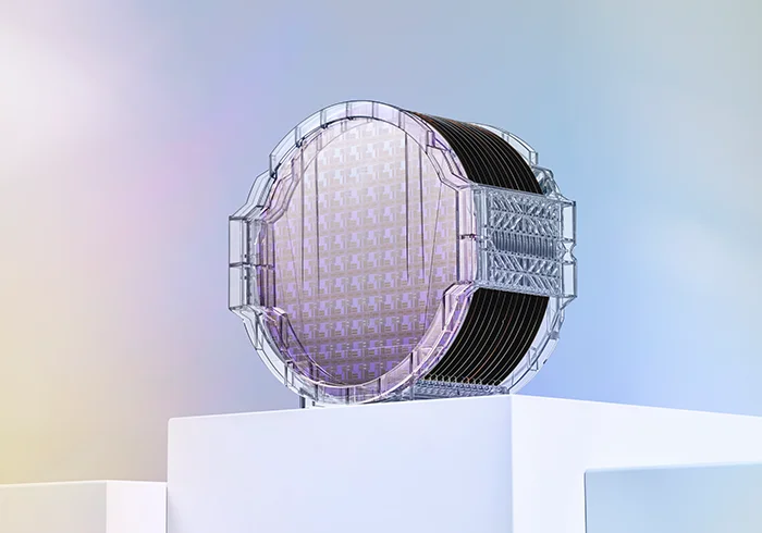
Coatings
Our service includes a variety of coating options to optimally prepare your wafers for their specific applications:
- Thermal Oxidation:
Wet oxidation (100 nm to 15,000 nm)
Dry oxidation (10 nm to 300 nm)
Chlorinated dry oxidation (10 nm to 300 nm) -
Silicon Nitride Coatings:
LPCVD Nitride (double-sided coating): Stoichiometric, Low Stress, Super Low Stress
PECVD Nitride (single-sided coating): Stoichiometric, Low Stress● Additional Coatings:
Titanium (Ti), Titanium Nitride (TiN), Gold (Au), Chromium (Cr), Aluminum (Al, AlCu), Copper (Cu), Nickel (Ni), Tantalum (Ta), Tungsten (W), Silicon Carbide (SiC), Silicon Nitride (SiN), and more.
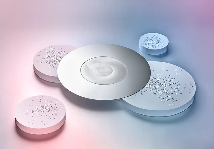
Reclaim-Wafer
Reclaim wafers offer a cost-effective way to reuse silicon substrates. The process includes the removal of coatings through etching and polishing, followed by a final quality inspection.
Process Steps:
- Inspection: Pre-sorting by type, thickness, and resistivity.
- Processing: Etching, polishing, and cleaning.
- Quality Inspection & Packaging: Secure double packaging and labeling.
To support lifecycle management, we also offer laser marking services and new silicon wafers as replacements for reclaim fallouts.
Wafer Thinning
We provide precise wafer thinning for various wafer sizes:
- 2″, 3″, 4″ Si wafers: Down to 10-20 µm
- 6″ and 8″ Si wafers: Down to 50 µm
- 12″ Si wafers: Down to 200 µm
Processing can be performed with single- or double-sided polishing, depending on your requirements.
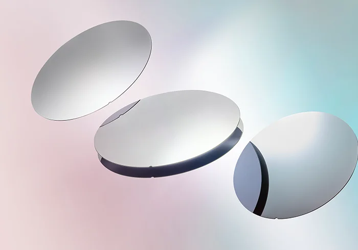
Laser Cutting
Our service ensures highly precise cutting processes, including:
- Diameter reductions and custom geometric cuts: According to SEMI standards or your specific requirements.
Laser Marking
For clear and precise wafer identification, we offer:
-
Engravings in vector or dot-matrix formats
-
Engraving depths ranging from 4 µm (Soft Laser Mark) to 60 µm (Hard Laser Mark)
Your custom solutions
Our service portfolio provides you with tailor-made solutions for seamless process integration and the highest quality standards.
Feel free to contact us to learn more about our custom services or our range of wafers.