


Semiconductor Outlook 2026: Navigating Growth and Opportunity
13. February 2026
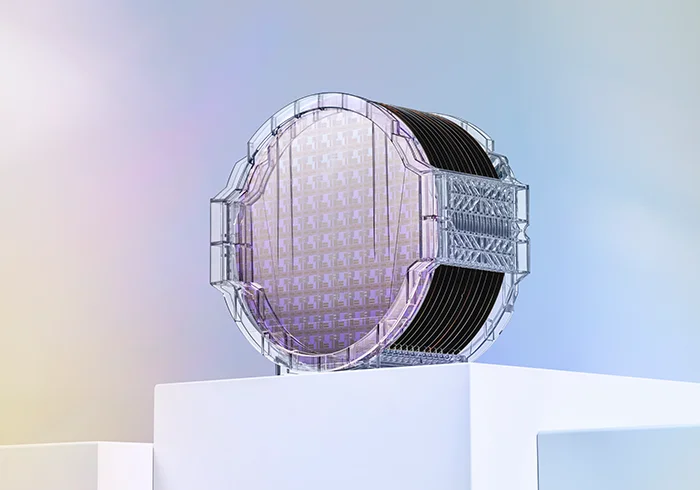
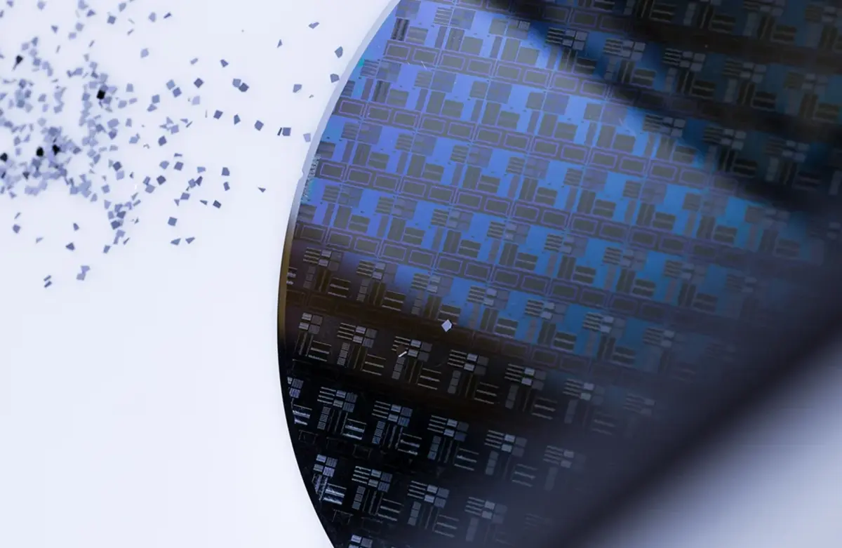
What 3nm Design Challenges Mean for Wafer Sourcing
7. April 2026
As semiconductor technology advances into the 3nm node, chip development is facing a new reality: scaling is no longer just a technical challenge—it is increasingly an economic one.
While innovations such as AI acceleration and multi-die architectures dominate industry discussions, a more fundamental issue often remains overlooked: the declining return on advanced-node scaling.
What Is the 3nm Pessimism Wall?
At 3nm, many design teams encounter a growing gap between theoretical performance gains and actual silicon results. A key reason is the accumulation of excessive clock margins, often reaching 25–35% of the total clock period.
This phenomenon, known as the “Pessimism Wall,” is not driven by physical limitations, but by conservative design methodologies.
To ensure reliability, factors such as voltage variation, jitter, and aging are evaluated separately and combined using worst-case assumptions. While each factor is valid, their cumulative effect leads to significant over-design.
Why It Matters
This structural over-margining has direct business implications:
- Higher power consumption: Clock networks represent a major share of total chip power. Unnecessary margin increases energy usage
- Lost performance potential: Recovering margin can directly translate into higher clock speeds and better product positioning
- Increased die size and cost: Over-design requires larger layouts and more complex routing
- Hidden reliability risks: Broad guard bands may mask real electrical issues instead of addressing them
In high-volume semiconductor markets, these effects can result in substantial financial losses and reduced competitiveness.
Root Cause: Methodology, Not Physics
The pessimism wall arises because modern design flows rely heavily on abstraction. Instead of resolving real electrical interactions, traditional timing analysis simplifies complex behaviors—especially at low voltages where transistor behavior becomes highly non-linear.
As a result, uncertainty is compensated by adding margin rather than improving accuracy.
A More Accurate Approach
To overcome these limitations, the industry is increasingly moving toward physics-based analysis methods. By evaluating real electrical interactions—across timing, power, jitter, and aging—design teams can:
- Reduce unnecessary safety margins
- Improve power efficiency
- Increase achievable performance
- Enhance long-term reliability
This approach allows engineers to align design assumptions more closely with actual silicon behavior.
What This Means for the Supply Chain
As design complexity increases, collaboration across the semiconductor supply chain becomes more critical. Reliable wafer quality, consistent specifications, and tight process control are essential to minimize variability and support advanced-node performance targets.
At ABC GmbH, we support semiconductor companies worldwide with high-quality silicon wafers and flexible sourcing solutions. By working with qualified manufacturing partners and offering tailored specifications, we help ensure a stable foundation for advanced-node applications.
Conclusion
At 3nm and beyond, success is no longer defined by adding more margin—but by removing unnecessary margin safely.
The pessimism wall is not a silicon limitation—it is a modeling challenge.
Companies that address it effectively will unlock performance, reduce costs, and gain a decisive competitive advantage.