


Pocket Wafer

Precision and safety with pocket wafers
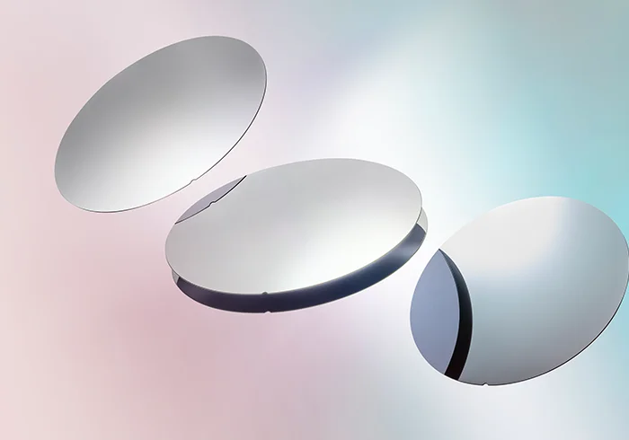
Pocket Wafers, also known as Carrier Wafers, are essential for the precise handling and processing of wafers of various sizes. They enable smaller wafers to be securely fixed, transported, and processed on existing equipment – efficiently, flexibly, and reliably.
ABC GmbH is your experienced supplier of high-quality Pocket Wafer made from monocrystalline silicon or alternative materials, customized to meet your specific requirements.
What are Pocket Wafers?
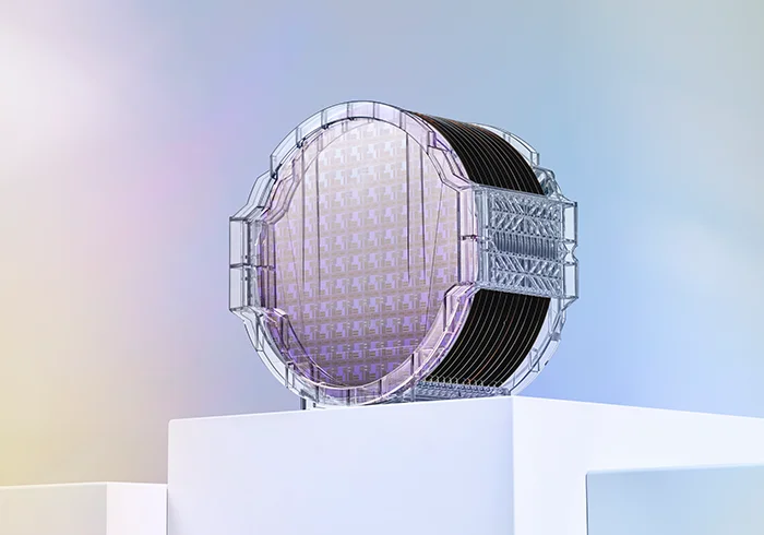
Pocket Wafers are carrier wafers with specially designed pockets that securely hold smaller wafers. This allows the processing of different wafer sizes on machines originally designed for larger wafers. We offer Pocket Wafer in various sizes, crystal orientations, and materials:
Our Specifications:
Wafer Sizes:
2" bis 12"
Crystal Orientations:
<100>, <110>, <111>
Materials:
Silicon (monocrystalline, multicrystalline), Ceramics (e.g., Al₂O₃), Quartz, sapphire, and other options
Pocket Wafer – Innovative Lösungen für Miniaturisierung und Flexibilität
How do Pocket Wafer work?
With increasing miniaturization, smaller wafers must be processed on machines designed for larger dimensions. Pocket Wafers solve this issue through:
- Pocket Structure: Precisely engineered pockets securely hold smaller wafers.
- Stable Fixation: Smaller wafers are positioned securely and precisely during processing.
- Process Compatibility: Various sizes can be processed on existing equipment.
What types of Pocket Wafer do we offer?
We provide Pocket Wafers tailored to your exact requirements:
Specifications:
Standard pockets or custom designs based on your needs
Material Variety:
Silicon, ceramics, quartz, sapphire, and more
Additional Features:
Grooves, holes, or rectangular pockets for specialized applications
Even for the most demanding requirements, we offer the ideal solution. Contact us for a personal consultation!
Benefits of Pocket Wafer
Take advantage of the many benefits of our Pocket Wafers:
- Cost Savings: Utilize existing machines with Pocket Wafers.
- Flexibility: Process wafers of various dimensions.
- Process Security: Secure transport and precise fixation.
Examples of standard Pocket configurations: 12” wafers with 8”-, 6”-, or 4”-pockets, 8” wafers with 6”- or 4”-pockets
Application areas for Pocket Wafer
Our Pocket Wafers are used across multiple high-tech industries:
- Automotive & Aerospace: Precision manufacturing of sensors and electronic components
- Mechanical Engineering: Optimization of microsystem technologies
- Optics & Watch Industry: Fixation of optical components for maximum precision
- Semiconductor Industry: MEMS, microprocessors, and sensors
- Medical Technology: Components for diagnostic and therapeutic devices
- Research & Development: Universities, Fraunhofer Institutes, and high-tech laboratories
Why choose ABC GmbH?
- Top Quality: High-quality Pocket Wafers made from tested materials
- Flexibility: Custom solutions tailored to your requirements
- Variety: Solutions for various wafer dimensions and materials
- Fast Delivery: Duty-paid shipments directly from the EU – reliable and fast
- Personal Consultation: A single point of contact for all inquiries
Our Pocket Wafers – Your Benefits:
Our pocket wafers offer clear advantages: cost savings through the use of existing equipment, flexible processing of different wafer sizes, and maximum process reliability through precise fixation.
Examples & future potential of Pocket Wafer
Application example:
A semiconductor manufacturer uses 12” Pocket Wafer to process smaller 6” wafer on existing equipment. Thanks to the specialized pocket structure, the smaller wafers are securely fixed and precisely processed - without the need for additional machinery. This saves costs and optimizes the use of existing equipment.
Future Potential:
New technologies such as 3D chip integration, component miniaturization, and semiconductor manufacturing for quantum computing are increasing the demand for flexible wafer solutions. Pocket Wafers play a crucial role in this evolution by:
- Enabling the precise fixation of tiny substrates
- Supporting the processing of various sizes and shapes on modern equipment
Optimize manufacturing processes, increase efficiency!
Optimize your manufacturing processes and increase your equipment efficiency!
Contact us for a non-binding quote or personalized consultation. We look forward to your Pocket Wafer inquiry.